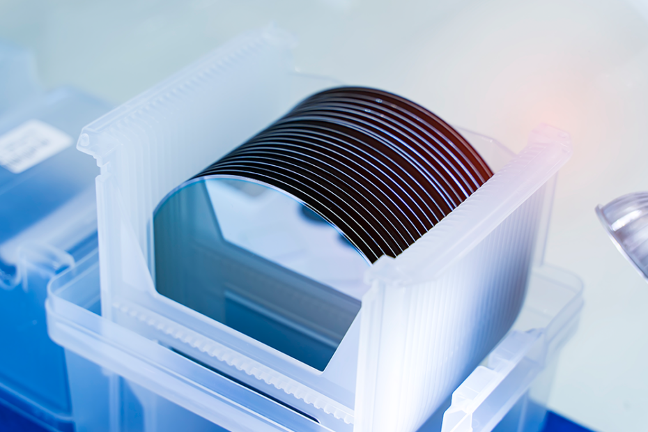
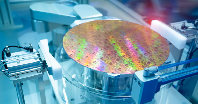
Think of silicon-based devices like microprocessors, integrated circuits, and memory chips. Yes, they are critical computer internal devices necessary to carry out the operations of the computer’s core processing unit. CMP or Chemical Mechanical Polishing plays a crucial role in manufacturing such silicon-based semiconductor devices.
Chemical-mechanical polishing is used when the goal is to eliminate surface materials. However, it is known as chemical-mechanical planarization when the goal is to flatten a surface. CMP Wafers have unique features designed for the effective removal of unwanted surface contaminants, homogeneity control, and defect elimination on a pretty tiny scale.
Advanced procedures for generating CMP wafers are nonetheless being developed to meet the increasingly stringent industry demands for microchip fabrication. These techniques provide improved accuracy and control over wafer planarization. The continued development of CMP wafers is essential for guaranteeing high-quality semiconductor manufacturing as demands rise and technology develops.
Role Of CMP Wafers In Semiconductor Technology
In the semiconductors industry, removing excess materials and generating a clean surface to construct ever-complex and smaller devices that power our contemporary digital world is critical. The semiconductor industry continues to search for smaller, faster, and more powerful electronic devices. To do this, manufacturers rely on cutting-edge technology that enables precise manufacturing using CMP wafers.
Planarization
Removal of topologies and smoothening of rough surfaces of pads and slurries is attained by planarization. Achieving planarization ensures a uniformly flat surface across the wafer as the purpose of CMP wafers. The planarization method eliminates the constant troubles the surface topography creates during further production procedures, like lithography and etching.
CMP wafers are essential for enabling consistent deposition and etching operations, which boost yield and performance by eliminating high and low areas on the wafer. The excellent precision and successful planarization rates of CMP wafers significantly contribute to the efficient production of semiconductor devices.
Optimization Of Integrated Processes
The CMP wafer technique helps improve the yield by allowing integrated optimization of processes in semiconductor production. Managing wafer surface parameters like roughness and topography to fine-tune future deposition and patterning processes.
Manufacturers may optimize process parameters like pressure, speed, slurry structure, and temperature with proper CMP wafer selection, resulting in performance uniformity across wafers and increased yield.
Defect Reduction
Chemical mechanical polishing helps remove the surface anomalies and unevenness of silicon wafers. Critical parameters, such as the rate of exfoliation and wafer imperfections, are directly impacted by the size distribution of the abrasive grainy particles.
CMP wafers can significantly boost yield by reducing defects on the wafer surface. Contamination, crystalline flaws, and particle-related problems significantly impact the manufacturing of semiconductors.
CMP wafers help to reduce faults and increase output by efficiently eliminating impurities. The elimination of undesirable materials is made possible by the closely regulated composition and surface quality of CMP wafers, which supports the decrease of defects overall.
Selection And Characterization Of CMP Wafers

Since high-grade Chemical Mechanical Polishing helps in the best results, choosing the best CMP wafer requires careful consideration of several parameters. Some parameters are wafer material, surface polish, hardness, the degree of roughness and flatness, density of defects, etc.
Identifying the best CMP wafer material with properties that match specific process requirements reduces interactions that cause faults and poor performance. Accurate characterization methods, such as atomic force microscopy and microscopy with scanning electrons, help evaluate the characteristics of chemical-mechanical polishing wafers and enable thoughtful selection.
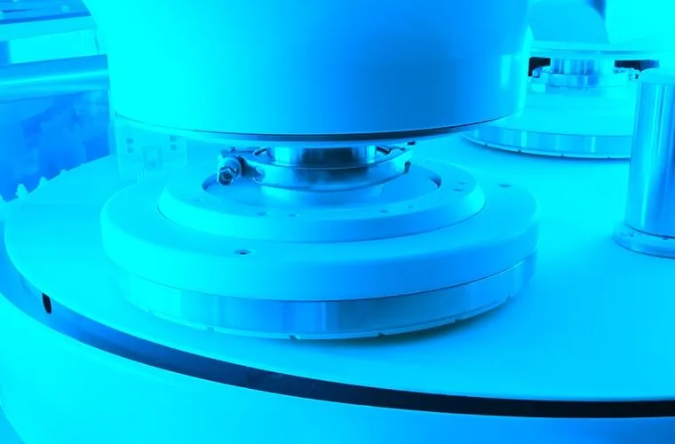
Film Removal
Commonly, CMP instruments use a revolving, extremely flat-leveled plate coated with a pad. It is critical to have a precise removal of surplus films and components in the semiconductor manufacturing process to yield results.
The wafer is kept in the proper horizontal position by a holding ring. Specialized characteristics of Chemical Mechanical Polishing wafers allow for efficient material removal, ensuring that the target film thickness is attained consistently across the wafer surface.
Their improved stability and selectivity enable the effective elimination of film layers while reducing surface erosion and maintaining the wafer structure’s integrity. The procedure (carrier) employs a vacuum during the loading and unloading of the wafer onto the tool to stop unwanted particles from accumulating on the wafer surface.
CMP wafers help improve process control by successfully eliminating undesirable films, which increases device yield.
Topography Control
Semiconductor product topography refers to the collection of fixed or coded structures that serve a three-dimensional pattern of coatings of conducting, insulating, or semiconducting material designed to perform an electronic function.
Strict surface topography control is essential for the production of semiconductors. Critical surface properties like step elevations, roughness, and pattern size are precisely controlled using chemical-mechanical polishing wafers.
CMP wafers help to achieve ideal planarity and smoothness by precisely polishing various materials and protecting and preventing probable circuit failures brought on by topographical problems.
Each arrangement denotes a depiction of a single layer of a semiconductor item in its various production steps. CMP wafers are crucial in assuring a greater yield of semiconductor chips by efficiently controlling surface topography during manufacture.
Wafer Upkeep And Durability
When it comes to maintaining a steady yield, it is critical to enhance CMP wafer maintenance processes. Cleaning and reconditioning must be performed regularly to provide optimal pad-wafer interactions, manage slurry dispersion, and avoid contamination.
In addition, routine evaluations, analysis of the surface, and replacement cycles can ensure Chemical Mechanical Polishing wafer productivity and lifespan. Adequate maintenance routines and monitoring systems provide long-term yield increases.
Conclusion
CMP wafers are a crucial component in increasing yield in the semiconductor industry. And since yield increase is a critical goal in semiconductor production, their essential responsibilities in planarization, defect reduction, film removal, and topographical control contribute considerably to obtaining maximum yield.
Given their precision, selectivity, and stability, CMP wafers are essential elements of the whole production process. As the sector of semiconductors advances, CMP wafers will continue to play a pivotal role in allowing the development of exceptionally well devised with increased yields.